Plasma Electronics Laboratory, Saga University
Plasma Electronics Laboratory
Functional thin film preparation by plasma processing
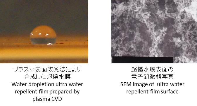
A. Water repellent thin film
Water repellency is required for the surfaces of all sorts of products in various industrial fields. For instance, the windshield must ensure a clear vision of the road under any meteorological conditions. That is, water-repellent glass enables safe driving by the reduction of glare in the rain, particularly at night, because water repellency brings beads up and rolls off raindrops. In this work, hard coating of water-repellent films being investigated with plasma processing.
B. High speed preparation of aluminum nitride thin films for high temperature piezoelectric sensor by novel plasma source
Piezoelectric sensor is widely used for various sensing systems. In especial,
it is well known that zirconium titanate (PZT) and barium titanate (BaTiO3) are useful piezoelectric materials.
The curie temperatures which loses piezoelectric characteristic in the case of PZT and BaTiO3 are 300 °C and 120 °C,
respectively. However, these temperatures are too low to use them as high temperature sensors for turbine and
automobile engine. PZT includes harmful atoms such as Pb. On the other hand, the curie temperature of
aluminum nitride (AlN) is about 1200°C and is the highest in all piezoelectric materials.
AlN is safety material for environment and is also expected as corrosion sensor.
In general, these materials are prepared with sintering method. However, AlN synthesized by
the sintering method is impossible to polarize. The thin film of AlN is effective for piezoelectric materials.
The thin film is synthesized by plasma sputtering.
A conventional deposition rate of AlN thin films prepared by magnetron sputtering is about 5 nm/min
and is too low to produce the required deposition thickness at short time of a few hour. In this work,
we have investigated to make the deposition rate faster with dual frequency plasma sputtering.
This work is being done under the joint research with Measurement Solution Research Center,
National Institute of Advanced Industrial Science and Technology (AIST).
Novel plasma processing apparatus
A. Development of high density plasma source with capacitive discharge and SEE for diamond-like carbon thin film preparation
Diamond-like-carbon (DLC) thin films such as a-C and a-C:H have
widespread applications as protective coatings in areas such as magnetic storage disks, car parts,
and biomedical coatings. Various deposition methods such as ion beam, sputtering, cathodic arc discharge,
plasma ion implantation, and plasma enhanced chemical vapor depositions (PE-CVD) have been proposed.
In these depositions, the most popular laboratory method is radio frequency (RF) capacitively coupled PE-CVD
using parallel-plate electrodes because the experimental arrangement is very simple.
However, plasma density is less than 1010 cm-3 and the deposition rate for methane gas is
a few tens of nanometers per minute. This is the main problem for RF capacitively coupled PE-CVD method. In order to
improve these results, some solutions based on: (1) high driving frequency and (2) precursors with
low ionization potential, such as acetylene have been proposed. These solutions have some disadvantages:
the conventional driving frequency is 13.56 MHz and the gas, such as acetylene, is not available in high purity
and possesses a substantial nitrogen impurity. In order to improve the growth rate of DLC films,
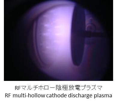
we proposed a method based on the effects of multi-hollow cathode discharge and high secondary electron emission in
a capacitively coupled discharge.
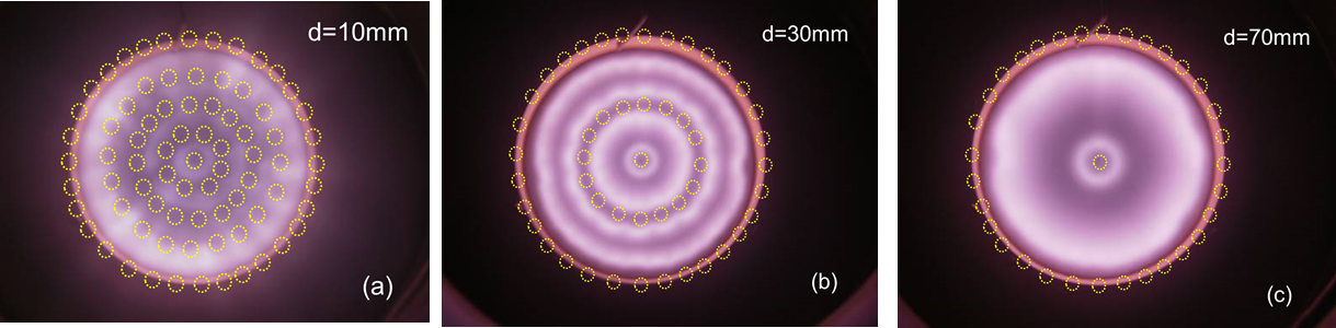
In this work, the influence of five multi-hollow arrangements in high-density RF plasma CVD on the uniformity of
the radial profile of the deposited film thickness has been examined.
B. Achievement of full erosion target in RF magnetron sputtering plasma for transparent conductive oxide film preparation
Transparent conductive oxide (TCO) thin films are widely used for the touch panel in mobile smart phone and tablet typed computer and solar panel.
The TCO thin films are prepared by the RF magnetron sputtering plasma which has a weak point. The weak point is that the target erosion ratio is very small, that is, 20 - 30 %.
The target material includes a rare metal such as indium. The full target erosion is required from a view point of utilization of resources.
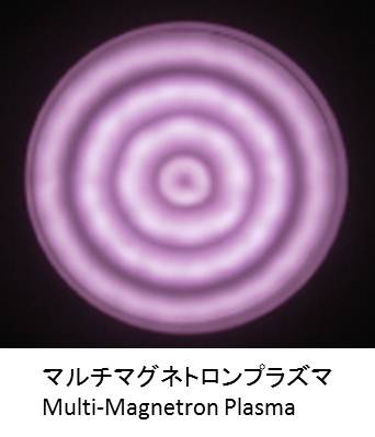
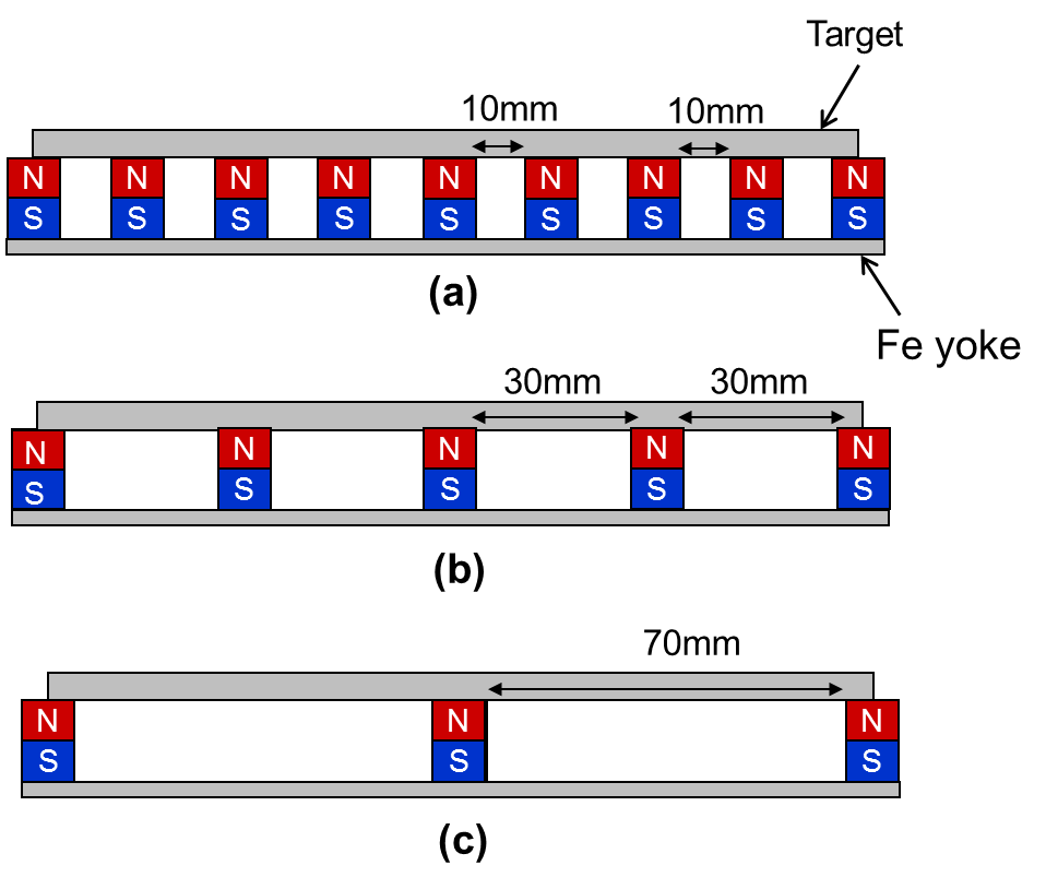
In our work, the novel sputtering plasma apparatus is developed by the optimization of magnets for the full target erosion.
As shown in right (various setups of magnets) and bottom (plasma images for various setups of magnets) figures, various typed magnetron plasmas are developed.
For the setup (b), the target erosion ratio has attained at approximately 60 %. Now, we are developing novel magnetron sputtering plasma with higher ratio.
C. Development of RF plasma sources for high-speed treatment by plasma processing
In order to develop an intelligent plasma source, various tries based on plasma physics have been applied. Effects of driving frequency, electrode material and hollow cathode discharge were investigated for production of high-density radio frequency plasma. A large diameter and uniform microwave plasma (about 30cm in diameter) has been produced with an annular slot antenna and ring-shaped permanent magnets. Energy distribution and 2-dimensional velocity space of ions have been measured in microwave plasma by means of energy analyzer.