Research SubjectsRESEARCH SUBJECTS
SiC, Nitride Power Device
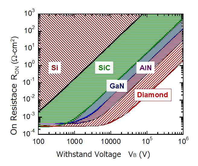
This figure shows on-site resistance (RON) and breakdown voltage (VB) of power transistors with various semiconductors. The on-site resistance
determines energy consumption during on state, and the breakdown voltage
determines the high limit of operation voltage, thus the output power.
The relation of the Ron and the VB is trade-off. The conventional silicon devices operate in green area.
In order to achieve both high energy efficiency and high output power,
we choose SiC (green), GaN (blue), AlN (violet), and diamond (red).
Therefore, we are focusing on high-quality SiC, GaN, AlN, diamond
and achieve p-type and n-type semiconductors and fabricate power transistors.
We will measure fundamental electric properties such as carrier mobility
and breakdown voltage, investigate fundamental physics of such wide-gap
semiconductors.
Next with molecular beam epitaxy (MBE), we fabricate atomic-scale
controlled GaN, AlN semiconductors.
Diamond Power Transistors
Diamond is called the ultimate power semiconductor because it intrinsically
has many superior physical properties over conventional semiconductors.
First, we will be making diamond single-crystal in a wafer size.
Then we grow p-type and n-type diamond semiconductors.
We will clarify electronic properties of diamond semiconductor and fabricate
diamond power transistors.
Wide-Gap Semiconductor Power-Control Circuit
Power-control circuit such as inverters operates in hundreds KHz
and MHz range, and therefore its switching characteristics are important
and is closely related with semiconductor’s electronic properties.
First, we will fabricate power-control circuit of wide-gap semiconductors
such as SiC and GaN, and diamond.
Diamond NV Center as Quantum Memory
Recently quantum computer and communication draw much attention.
Quantum computer can operate quantum information processing with 'quantum
bit'. It will solve complicated factoring algorithm much faster than conventional
computers.
NV center is nitrogen-vacancy complex in diamond crystal. Negatively-charged
NV center can be observed as light emission with a wavelength of 637 nm
zero-phonon line (ZPL) and electron captured by NV center has energy split
at 2.88 GHz and its energy is similar to energy required for quantum bit.
We will make nitrogen-doped diamond crystal best suitable for quantum
memory.
POWER ELECTRONICS LAB
(KASU LAB)
Honjo-machi, Saga 840-8502
Japan
TEL +81-952-28-8648
FAX +81-952-28-8648
E-mail kasu(at)cc.saga-u.ac.jp